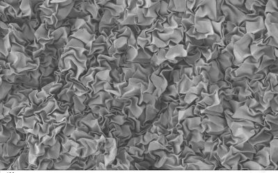
The reliable separation of some gases from others could be highly advantageous for a wide range of applications. For instance, it could help to produce hydrogen (H2) for fuel cells and chemical applications or to capture the carbon dioxide (CO2) emitted by industrial...
Nanophysics
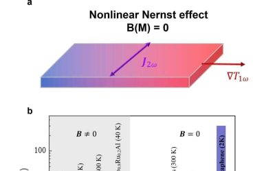
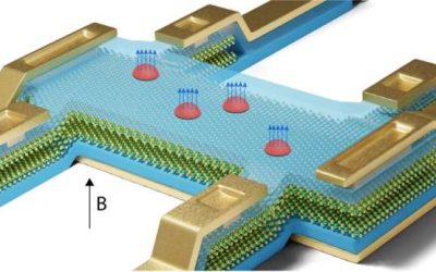
The first observation of a giant nonlinear Nernst Effect in trilayer graphene
The generation of electricity from heat, also known as thermoelectric energy conversion, has proved to be advantageous for various real-world applications. For instance, it proved useful for the generation of energy during space expeditions and military missions in...
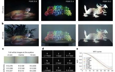
Single-layer waveguide display uses achromatic metagratings for more compact augmented reality eyewear
Augmented reality (AR), the technology that overlays digital content onto what users see around them in real-time, is now widely used in the retail, gaming and entertainment industries, as well as in some educational settings and learning environments. A key component...
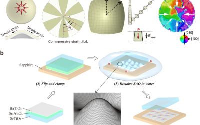
A recently realized ferroelectric topology in nanomembranes enables light field manipulation
Ferroelectrics are a class of materials that exhibit so-called spontaneous electric polarization, which is the separation of electric charges that can be reversed when an external electric field is applied to them. The dipole moments (i.e., pairs of equal and opposite...
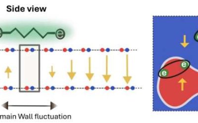
Domain wall fluctuations in 2D materials reveal a new mechanism of superconductivity
Two-dimensional (2D) van der Waals are made of atomically thin layers, held together by weak van der Waals forces. These materials have been the focus of numerous studies, as their unique properties make them ideal for studying various exotic and rare physical...
2D materials boost p-type transistor performance, paving way for future tech
After dominating the electronics industry for decades, conventional silicon-based transistors are gradually approaching their limits, which is preventing engineers from further reducing their size without affecting their performance. To continue advancing portable...
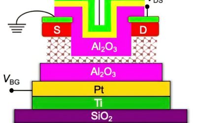
New method realize ohmic contacts in n-type MoS₂ transistors at cryogenic temperatures
Semiconducting transition metal dichalcogenides (TMDs) are a class of layered materials exhibiting unique optoelectronic properties that could be leveraged to develop transistors, sensors and other nanoelectronics. Despite their advantages, creating robust ohmic...
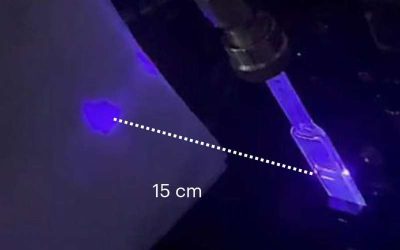
New blue light-emitting lasers leverage low-toxicity colloidal quantum dots
Blue lasers, lasers that emit a light beam with a wavelength between 400 nm and 500 nm, are key components of various technologies, ranging from high-resolution displays to printers, medical imaging tools and data storage solutions. A key advantage of these lasers is...
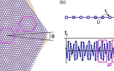
Quasiperiodicity changes the ground-state properties of 1D narrow-band moiré systems, study demonstrates
Moiré materials, such as twisted bilayer graphene, are materials generally formed by stacking two or more layers of 2D materials on top of each other with a small lattice mismatch. This slight mismatch creates a unique pattern known as the moiré pattern, which is...
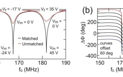
New varactor enhances quantum dot device measurements at millikelvin temperatures
The development of quantum computing systems relies on the ability to rapidly and precisely measure these systems' electrical properties, such as their underlying charge and spin states. These measurements are typically collected using radio-frequency resonators,...

